TEM Communications Driver
Software User's Guide
Curt Brune
GLAST Flight Software
- Table of Contents
- Background Documentation
- 1. Theory of Operation
- 2. Commanding
- 3. Event Taking
- A. Response FIFO
- B. Mini GLT
- C. Virtual AEM
- List of Tables
- 1. Background Documentation
- A-1. Wire Count
- B-1. Setting Flow Control
- List of Figures
- A-1. A two cell LATp packet
- B-1. Structure of the Trigger register.
- B-2. Structure of the trigger source mask in the Trigger Mask/Config register.
- B-3. Structure of the trigger message
- B-4. Structure of the initial event number and parity definition in the Trigger Mask/Config register.
- B-5. Structure of the Options register.
- C-1. I/O Lines for Virtual AEM setup.
- C-2. Structure of the Virtual AEM software driver.
- List of Examples
- B-1. Calorimeter Calibration Strobe
Background Documentation
This document builds upon the following documents:
| Document Title | Document Number |
|---|---|
| LAT VME Front-End Communication (Com) Board | LAT-DS-00226-D1 |
| LAT Inter-module Communications | LAT-TD-00606-D1 |
| Tower Electronics Module – A Primer | LAT-TD-00605-D1 |
| ACD Electronics Module – A Primer | LAT-TD-00639-D1 |
| ACD-AEM Interface Control Document | LAT-SS-00363-D9 |
Table 1. Background Documentation
Chapter 1. Theory of Operation
Commanding and taking event data from the TEM requires two LAT COMM I/O Boards – one for command I/O with the TEM and one for triggering and event read out. The software driver provides a C language funtional interface for creating opaque handles to the Command/Response COMM Board (hereafter GTEM) and to the mini-GLT COMM Board (hereafter GGLT). These handles are passed as arguments to subsequent methods appropriate to each type of COMM Board (see Chapter 2 and Chapter 3).
Initializing the sytem for running consists of initializing the driver handles for the two LAT COMM I/O Boards, configuring the GTEM registers and configuring the GGLT registers.
1.1. Initializing Driver
Before initializing the driver handles environment variables must first be set.
1.1.1. Environment
The driver expects to operate in a VxWorks hosted environment with a VME bus interface. Several parameters specific to VME are passed to the driver using VxWorks envinronment variables. These variables include the VME address, VME IRQ level and VME IRQ vector for each LAT COMM I/O Board
In addition to the VME parameters the LATp source address is also specified as an environment variable.
The following is an excerpt from a VxWorks startup script, specifying the required environment variables:
  # global "ENV" variables
  # LATpSourceAddr -- arbitrary 5 bit integer
  putenv ("GTEM_LATP_SOURCE_ADDR=5");

  ### Command Response COMM Board Setup ###
  # VME physical address -- corresponds to jumper block on
  # COMM I/O Board, connector SW1 and SW2.
  putenv ("GTEM_VME_ADDRESS=0x08000000")

  # VME IRQ level -- make sure does not conflict with any other VME modules
  putenv ("GTEM_VME_IRQ_LEVEL=4")

  # VME IRQ vector
  putenv ("GTEM_VME_IRQ_VECTOR=200")
  ### End Command Response COMM Board Setup ###

  ### mini-GLT COMM Board Setup ###
  # VME physical address -- corresponds to jumper block on
  # COMM I/O Board, connector SW1 and SW2.
  putenv ("GGLT_VME_ADDRESS=0x08800000")

  # VME IRQ level -- make sure does not conflict with any other VME modules
  putenv ("GGLT_VME_IRQ_LEVEL=5")

  # VME IRQ vector
  putenv ("GGLT_VME_IRQ_VECTOR=220")
  ### End mini-GLT COMM Board Setup ###
|
1.1.2. Debugging Output
The driver can log debugging information to the serial line of the MVME2304 processor board. The verbosity of this output is controlled by the logLevel argument of the gtOpen() function. logLevel can take the values LOG_DEBUG, LOG_INFO, LOG_WARN, LOG_ERROR or LOG_NONE. It is reccommended to use a value of LOG_ERROR for normal running.
1.1.3. Allocating Handles
Storage for the GTEM and GGLT handles must first be allocated before attempting to open the handles. Use the gtSizeOf() and ggSizeOf() functions to determine how much storage to allocated.
Once allocated the handles can be opened with for the are created using the gtOpen() and ggOpen() functions. The following code snippet shows how to allocate a GTEM handle:
  gtemHandle gt = NULL;

  /* create gtemHandle gnatHandle */
  gt = (gtemHandle)malloc(gtSizeOf());
  if ( !gt) {
    return NULL;
  }
  status = gtOpen( gt, (LOG_level)logLevel);
|
An analogous calling sequence is used to allocate a GGLT handle using the functions ggSizeOf() and ggOpen().
1.2. Initializing TEM Hardware
After initializing the software driver the next step is to initialize the GGLT followed by initializing the GTEM.
1.2.1. Initializing the GGLT
Before configuring the GGLT, the GGLT module must be initialized. This is simply done as follows:
/* init the GGLT module */ status = ggInit( gg); |
Next configure the trigger masks of the GGLT. The following code enables the internal trigger source, while disabling all other trigger sources.
  /*
     set trigger to disable all trigger sources, except for the
     internal self trigger.  Also make sure the THROTTLE is disabled.
  */
  status = ggSetTrgMask( gg,
			 TRG_DISABLE_THROTTLE | TRG_DISABLE_3_IN_A_ROW | TRG_DISABLE_CAL_HIGH |
			 TRG_DISABLE_CAL_LOW  | TRG_DISABLE_EXT_TRG );
|
Next configure the bits of the trigger message you wish to send. The following code configures the trigger message to do zero supression, auto range data, no calibration strobe and no TACK signal. The destination and marker are arbitrarily set.
  /*
     set dynamic part of trigger message

     default configuration has zero supression turned on and 4range
     data turned off.

  */
  status = ggSetTrgDest( gg, 5);
  status = ggSetTrg4range( gg, 0);
  status = ggSetTrgZeroSupress( gg, 1);
  status = ggSetTrgCalStrb( gg, 0);
  status = ggSetTrgTACK( gg, 0);
  status = ggSetTrgMarker( gg, 0);
|
Next configure the front end hardware using the GTEM handle.
1.2.2. Initializing the GTEM
Before configuring the GTEM, the GTEM module must be initialized. This is simply done as follows:
/* init the GTEM module */ status = gtInit( gt); |
The configuration of the GTEM is highly dependent on the subsystem in question. The following code configures the GTEM for taking Calorimeter data. Other subsystems will program the GTEM differently ( see Chapter 2 ).
  /* clear TEM statistics register */
  status = gTEMload( gt, temId, TEM_REG_CMD_RSP_STATS, 0x0);

  /* clear TEM status register */
  status = gTEMload( gt, temId, TEM_REG_STATUS, 0x0);

  /*
     Configure TEM data masks register

     Default configuration:
       Diagnostic            -- disabled
       CAL Cable Controllers -- enabled
       TKR Cable Controllers -- disabled
  */
  temREG_DataMasks.ui = 0x0;
  temREG_DataMasks.bf.diagnostic = 0;
  temREG_DataMasks.bf.cal = 0x0;
  temREG_DataMasks.bf.tkr = 0xFF;
  status = gTEMload( gt, temId, TEM_REG_DATA_MASKS, temREG_DataMasks.ui);

  /* large TEM timeout */
  temREG_Config.ui = 0x0;
  temREG_Config.bf.cableTimeout = 0xFFF;
  status = gTEMload( gt, temId, TEM_REG_CONFIGURATION, temREG_Config.ui);

  /* enable output in our GCCCs */
  gcccREG_Config.ui = 0x0;
  gcccREG_Config.bf.controllerOutEnable = 1;
  status = gGCCCload( gt, temId, BROADCAST_ADDRESS, GCCC_REG_CONFIGURATION, gcccREG_Config.ui);

  /* disable all GCRCs in all GCCCs */
  status = gGCCCload( gt, temId, BROADCAST_ADDRESS, GCCC_REG_LAYER_MASK_0, 0xFFFFFFFF);
  status = gGCCCload( gt, temId, BROADCAST_ADDRESS, GCCC_REG_LAYER_MASK_1, 0xFFFFFFFF);

  /* large timeouts for all GCCCs */
  gcccREG_EventTimeouts.ui = 0x0;
  gcccREG_EventTimeouts.bf.timeout = 0x3FF;
  status = gGCCCload( gt, temId, BROADCAST_ADDRESS, GCCC_REG_EVENT_TIMEOUTS, gcccREG_EventTimeouts.ui);
|
1.3. Event Taking Configuration
Event taking is an asynchronous activity. Before taking event data the GGLT driver requires two user supplied call back functions. One is a memory allocator and the other is an event handler.
1.3.1. Memory Allocation Callback
When an event is detected the GGLT driver calls a user supplied memory allocator to retrieve storage for the event. The function signature of the memory allocator is identical to malloc(). This allows the user to manager memory however they want.
Currently the driver requests 4K of memory for each event, but this is subject to change. The following code shows a very simple implementation of a memory allocator and how to set it in the GGLT driver.
  /*
     event handling memory allocator

     Current implementation is a simple wrapper around malloc().
     Good enough for debugging a couple events at time.

  */
  static void *evAlloc( size_t nBytes) {

    unsigned int *p;
    p = (unsigned int *)malloc(nBytes);
    printf("evAlloc: allocated %d bytes @ addr 0x%08x\n", nBytes, (unsigned int)p);
    return (void *) p;
  }

  ...

  /* set memory allocator callback */
  status = ggEvtSetAllocate( gg, evAlloc);
|
1.3.2. Event Handler Callback
After allocating storage the event the GGLT driver reads the event data from the LAT COMM I/O Board and into the allocated buffer. Next the GGLT driver calls a user supplied event handler, passing in the buffer, the buffer length in bytes and a status code.
A sample event handler is shown below that simply prints the event data as a list of unsigned ints. Note that the return value from the event handler controls further event processing. If the return value is non-zero no further event processing will occur.
  /*
     the return value of evHandler controls further event processing.
     returning any value other than G_OK will terminate event processing
     and cause the ggEvtWait() function to return (returning non G_OK
     value returned by evHandler).
  */
  static int evHandler( void *buf, size_t nBytes, int status) {

    int i;
    unsigned int *pEv = (unsigned int *)buf;

    for ( i = 0;  i < nBytes/sizeof(unsigned int) ; i++) {
       printf("evHandler(): \t event payload 32-bit word 0x%08x, %d\n", *pEv++, i);
    }

    ...

  /* set event handler callback routine */
  status = ggEvtSetHandler( gg, evHandler);
|
A simple ASCII based event decoder is provided by the EVUT CMX package.
1.3.3. Event Loop
Once the call back functions are in place the user is ready to enter the event processing loop. The event processing loop continually processes events until the event handler ( see Section 1.3.2 ) returns a non-zero value. This allows the user to control the termination of event processing in the event handler callback.
Entering the event processing loop looks like:
/* enter event processing loop */ status = ggEvtWait( gg); |
The function ggEvtWait() does not return until the event handler returns a non-zero value. The value returned by ggEvtWait() is the same non-zero value that the event handler returned.
1.4. Triggering
The GGLT interface provides an internal self trigger routine. After all the hardware is configured and the event processing loop is running the user can call the self trigger from another VxWorks task. Calling the self trigger looks like this:
status = ggSelfTrg( gg); |
Calling this function begins the following sequence of steps:
A trigger message is formed in the GGLT using the current trigger message configuration. This message includes a new event number.
The trigger message is sent from the GGLT to the TEM board.
The TEM decodes the trigger message and forwards it on to the appropriate electronics ( cable controllers, front end electronics, etc... ).
The front end electronics trigger and send data back to the TEM
The TEM packages the event data and sends it to the GGLT LAT COMM I/O Board.
The GGLT calls the user supplied memory allocator for a buffer to hold the event data.
The GGLT reads the data from the LAT COMM I/O Board and stores it the buffer.
The GGLT calls the user supplied event handling routine, passing in the event buffer.
The event handler routine processes the event data in a user defined way.
The event handler decides whether to continue processing more events by returning a non-zero value or not.
In between triggers the user is allowed to change the GTEM configuration or the GGLT configuration.
Appendix A. Response FIFO
This appendix relies heavily on the LAT VME Front-End Communication (Com) Board and the LAT Communications documents mentioned in the Preface ( Background Documentation ). Please read these documents before reading this section.
The LAT VME Front-End Communication (Com) Board document describes the LAT COMM I/O Board, including its operation and VME registers. The important details for this appendix are:
The VME register for the response FIFO is 32-bits wide.
The physical FIFO is only 18 bits wide, thus only the 18 LSB of the VME register are relevant.
The LAT COMM I/O Board can raise a software configurable interrupt when data is ready in the response FIFO.
The LAT Communications document describes a bit serial wire communications protocol (here after LATp) that provides a uniform mechanism for the exchange of any and all information within the LAT.
This appendix specifies a data format for the response FIFO of the LAT COMM I/O Board. The format of the data in the response FIFO will follow LATp. The specification is central to the VHDL coding of the COMM Board's FPGA and facilitates read out by flight software.
A.1. Response FIFO Data Format
A.1.1. LATp Overview
A brief overview of LATp is presented next. Read LAT Communications for more details.
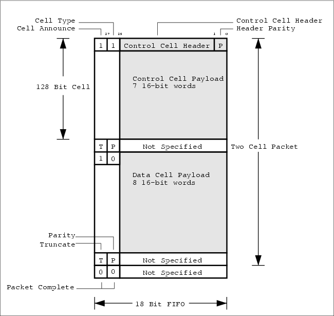
In LATp data is transmitted and recieved in the form of a packet, which consists of 1 control cell followed by 0 or more data cells. A packet always has a control cell.
Preceeding every cell on the wire is a two-bit field called the delineator. If the MSB of the delineator is set, a cell is assumed to immediatedly follow the delineator. The LSB of the delineator indicates the type of the following cell – control cell (1), data cell (0).
Cells are 128 bits long regardless of type. Following every cell is a truncate bit (see Flow Control, Section A.1.3 ) and a parity bit, containing the odd parity of the preceeding 129 bits.
Control cells consist of a 16-bit header, one bit of which is the odd parity of the header, followed by 112 bits (seven 16-bit words) of payload.
A packet may optionally have data cells following the control cell. Data cells consist of 128 bits (eight 16-bit words) of payload.
An isolated LATp packet consisting of 1 control cell and 1 data cell is shown in Figure A-1. The following sections describe the parity and 16-bit word mapping depicted in Figure A-1 as it would appear in the 18-bit wide response FIFO.
 | An isolated LATp packet ( no other packets immediatedly following ) must be followed by a word of all zeros in the response FIFO. In particular the Cell Announce and Cell Type bit fields must be set to zero. This indicates that the packet is complete. In the case of back to back packets the word of all zeros would not be needed as the Cell Announce and Cell Type bit fields of the next packet would both be set indicating the start of a new packet. Again, see LAT Communications for examples of back to back packets. |
A.1.2. Mapping LATp to Response FIFO
LATp is a bit serial wire protocol that must be mapped into multiple 18-bit chunks to fit in the response FIFO of the LAT COMM I/O Board.
It is straight forward to store a 128-bit cell as eight 16-bit words into the 16 LSB of the FIFO. The two MSB of an 18-bit FIFO word can also be used to store the two delineator bits, truncate bit and cell parity error bit as follows:
The two-bit delineator will accompany the first 16-bit word of a cell in the response FIFO as the two MSB. This is indicated in Figure A-1 as the Cell Announce and Cell Type bit fields.
The truncate bit and the cell parity error bit will occupy the two MSB of the 18-bit FIFO word immediately following the last (eighth) 16-bit word of a cell in the response FIFO. The 16 LSB of this FIFO word are unspecified. Refer to Figure A-1 for details.
| The two MSB of the 18-bit FIFO word are unspecified, except for:
|
A.1.3. Flow Control
LATp has the concept of flow control between transmitters and recievers – for complete details read LAT Communications. To sumamrize the truncate bit ( see Figure A-1 ) is set by the transmitter when the following conditions are all true
The transmitter detects busy while transmitting a cell AND
The cell is not the last cell in the packet.
As a consequence in the command response protocol we will never see the truncate bit set because the response packet consists of only 1 control cell. During event taking, however, we may see a set truncate bit because event packets consist of multiple cells.
| Sending data with flow control requires two wires, one for the transmitter to send data and one for the reciever to assert busy. |
A.2. Interrupt on Packet Ready
When a complete packet, consisting of 1 control cell and zero or more data cells, is ready in the response FIFO the LAT COMM I/O Board will assert a VME interrupt. The LAT COMM I/O Board already has an interrupt configuration register so that flight software can configure which interrupt is asserted on packet ready.
On interrupt flight software will service the interrupt and read the LATp packet from the FIFO.
A.3. Wire Count
The LAT COMM I/O Board has 18 output wires ( or channels ) and 18 input wires for sending and recieving signals. From the prespective of the LAT COMM I/O Board the needed channels are shown in Table A-1. For channel # NS stands for Not Specified indicating hardware is free to choose any channel number.
Appendix B. Mini GLT
This appendix relies heavily on the LAT VME Front-End Communication (Com) Board and the LAT Communications documents mentioned in the Preface ( Background Documentation ). Please read these documents before reading this section.
This appendix specifies VME registers for the LAT COMM I/O Board when it is used as a mini-GLT for triggering and event data taking. By introducing a set of VME registers software can control the trigger sources and specify the bit fields of trigger messaged constructed by the LAT COMM I/O Board.
B.1. Triggering
The trigger decision is the result of the trigger calculation using the trigger input sources. The trigger sources and trigger calculation are covered in this section.
B.1.1. Trigger Sources
The LAT COMM I/O Board will support 5 trigger sources:
3-in-a-row from the TEM
CALHigh from the TEM
CALLow from the TEM
external trigger line
internal trigger source (VME Register)
The LAT COMM I/O Board input lines for the 3-in-a-row, the CALHigh and the CALLow trigger sources are documented elsewhere ( see Section A.3).
The external trigger source is connected to the front panel of the LAT COMM I/O Board using connector J4 with label TST0.
The internal trigger source is activated using the Trigger register, shown in Figure B-1. Writing any value to this VME register will create a one shot trigger source as input to the trigger calculation ( see Section B.1.2 ).

B.1.2. Trigger Calculation
A bit mask, contained in the Trigger Mask/Config register, allows software to select which combination of trigger sources are active. The bit mask occupies bits 20 through 24 of the Trigger Mask/Config register, as shown in Figure B-2.
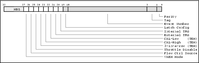
The bit mask is mask enabled so that a value of all zeros means all trigger sources are enabled. To disable a trigger source set the corresponding bit of the Trigger Mask/Config register.
In addition to the trigger sources the TEM provides a Throttle signal that inhibits triggering when high. The LAT COMM I/O Board will dedicate an input line to the Throttle signal for use in the trigger calculation ( see Section A.3).
The Throttle Disable bit of the Trigger Mask/Config register determines if the Throttle signal is considered in the trigger calculation. This allows for testing what happens when the Throttle signal is ignored. If the bit is set then the Throttle signal is ignored when calculating a trigger.
B.1.3. Event Data Flow Control
The mini-GLT can assert flow control back to the TEM during event taking. How flow control is asserted depends on the Flow Ctrl Source bit of the Trigger Mask/Config register shown in Figure B-2. Table B-1 describes how this bit affects the flow control line.
B.1.4. Virtual AEM Mode
The mini-GLT operates as a Virtual AEM when the Virtual AEM mode bit is set in the Trigger Mask/Config register ( see Figure B-2). In this mode the input serial data is processed differently than in normal GGLT running. See Appendix C for more about the Virtual AEM.
B.2. Trigger Message
The structure of a trigger message is illustrated in Figure B-3.
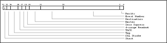
At a high level the trigger message consists of two parts: the dynamic high order 16 bits that vary from event-to-event and the low order 16 bits which are mostly static due to the slowly changing event number.
B.2.1. Trigger Mask/Config register
At the start of a data taking run software specifies the initial event number, initial tag and the definition of parity ( either even or odd ) in the 18 LSB of the Trigger Mask/Config register, as shown in Figure B-4.
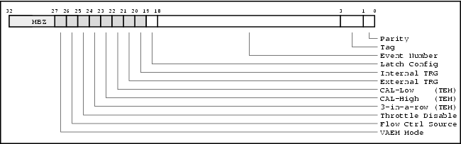
Figure B-4. Structure of the initial event number and parity definition in the Trigger Mask/Config register.
At the start of a data taking run software informs the hardware to latch the initial event number, initial tag and parity definition by transitioning the Latch Config bit (bit 19) of the Trigger Mask/Config register from 0 to 1. These parameters will be constant for the duration of the data taking run.
For each trigger message in a data taking run the LAT COMM I/O Board board will generate a monotonically increasing event number using the 15-bit event number and 2-bit tag of the Trigger Mask/Config register as the initial seed. These fields specify what the first event number will be.
On overflow the event number will wrap around to zero.
The bit labeled parity in the Trigger Mask/Config register controls whether to use even parity (bit set) or odd parity (bit clear). This allows software to force parity errors for testing purposes.
Using the Trigger Mask/Config register the LAT COMM I/O Board will construct the 16 LSB of a trigger message.
B.2.2. Options register
The dynamic component the trigger message resides in another VME register, the Options register. The Options register is mapped out in Figure B-5. These bit fields may be frequently updated by software on a per event basis.
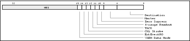
The LAT COMM I/O Board will use this register to construct the 16 MSB of a trigger message.
The ExtEventRO bit controls whether trigger messages generated by the COMM board in response to external trigger sources will include the current values for the CalStrobe and TACK bits.
If the ExtEventRO bit is set then trigger messages generated by the COMM board in response to external trigger sources will have the CalStrobe and TACK bits cleared, i.e. a normal event read out trigger is sent.
If the ExtEventRO bit is clear then trigger messages will contain the values of the CalStrobe and TACK bits currently assigned in the Options register. Setting the ExtEventRO bit allows one to take event data by sending a naked CalStrobe trigger message – the much sought after self triggering mode.
Example B-1. Calorimeter Calibration Strobe
Consider the case of the CAL where a naked CalStrobe trigger message is used for self triggering. In this case the Options register is programmed with the CalStrobe bit set, the TACK bit clear and the ExtEventRO bit set.
The internal software trigger is then initiated, resulting in a CalStrobe trigger message. This message raises the high energy CAL trigger signal coming from the CAL front ends, which is an external trigger source. With the ExtEventRO bit set the LAT COMM I/O Board will then send down an event readout trigger message upon seeing the high energy trigger signal. This results in a regular event read out initiated by a naked CalStrobe.
If the ExtEventRO bit had been clear the LAT COMM I/O Board would have send down another CalStrobe trigger message, since the CalStrobe bit is set in the Options register.
B.2.2.1. Virtual AEM Data Mode
When the mini-GLT operates as a Virtual AEM the Virtual AEM Data Mode bit of the Options register controls the expected input data format. When set the data is expected to be in ACD event data format. When this bit is clear the data format is expected to be that of a response to a ACD command. See Appendix C for more about the Virtual AEM.
Appendix C. Virtual AEM
This appendix relies heavily on the LAT VME Front-End Communication (Com) Board, the LAT Communications and the ACD Electronics Module documents mentioned in the Preface ( Background Documentation ). Please read these documents before reading this section.
This appendix describes the Virtual AEM, a combination of a specialized LAT COMM I/O Board and driver software that simulates the functionality of a real AEM electronics board. The Virtual AEM will be used in the I&T Test Stands for the ACD until the real AEM board becomes available.
C.1. Hardware Setup
In the Virtual AEM setup a single LAT COMM I/O Board communicates directly with ACD's FREE electronics module as shown in Figure C-1.
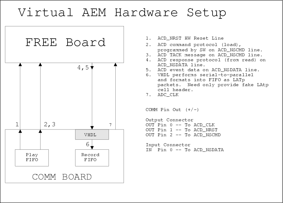
The FREE board requires 3 input signals and 1 output signal as shown in Figure C-1.
C.1.1. Required Hardware
A complete test stand for the Virtual AEM consists of the follow hardware:
1 LAT COMM I/O Board with firmware version 2.3 or later
1 FREE simulator board
1 customized cable, connecting COMM board and FREE board.
1 Motorola SBC
1 VME crate
1 I&T test stand PC workstation with SCL
C.1.2. Input Signals
The input signals consist of clock, reset and command signals labeled ACD_CLK, ACD_NRST and ACD_NSCMD respectively in Figure C-1.
| The ACD_NSCMD signal is used for both commanding and triggering. |
The driver software will program these three input signals by loading the playback FIFO of the LAT COMM I/O Board appropriately. No additional hardware(VHDL) changes are necessary.
C.1.3. Output Signals
The single data output signal is labeled ACD_NSDATA in Figure C-1. This signal carries command response data and event read out data – we need a mechanism for differentiating these two forms of data.
We propose adding a new bit to an existing VME register ( perhaps the Options register ) called the "Virtual AEM Data Mode" bit. Software will program this bit according to what type of data is expected.
Software requests that the data on the ACD_NSDATA line be formatted by hardware in to LATp packets into the record FIFO of the LAT COMM I/O Board. See Figure A-1. This includes:
Recognize the start bit on ACD_NSDATA.
Add the cell announce and cell type bits to the record FIFO.
Add a dummy LATp cell header word to the record FIFO. Software does not care what the cell header content is so long as the cell header parity bit is correct.
Format the serial data stream from ACD_NSDATA into parallel 16-bit words in the record FIFO as cell payload. For response data the payload will fit in a single cell – for event data it will be necessary to span LATp cells. See Section C.1.3.1 and Section C.1.3.2 below.
For every cell calculate and set the cell truncate and cell parity bits correctly.
Upon reading a complete packet hardware will fire an interrupt.
C.1.3.1. Command Data
When set, the "Virtual AEM Data Mode" bit indicates that data arriving on ACD_NSDATA is in the format of a fixed length response to a command (see "ACD Front-End Electronics to AEM ICD", section 7.5.1) . The data length is 32 bits, including the start bit.
This data shall appear as 2 16-bit words in the cell payload.
C.1.3.2. Event Data
When clear, the "Virtual AEM Data Mode" bit indicates that variable length event data is expected on the ACD_NSDATA line. In this mode hardware will need to decode the "Zero Supression Bits" in order to determine the end of the event data ( see "ACD Front-End Electronics to AEM ICD", section 7.5.2). The event data consists of a fixed 39 bit header (including start bit) followed by 0 to 18 15-bit words, as determined by the number of bits set in the "Hit Map Bits".
The 39-bit header will be padded with 9 MBZ bits and stored as 3 16-bit words in the cell payload. Each 15-bit PHA value will be padded with 1 MBZ bit and stored as a 16-bit word in the cell payload.
C.2. Simulation Fidelity
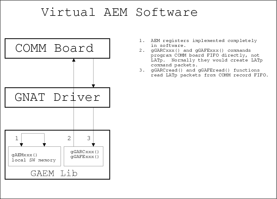
The following sections cover the details of the simulation fidelity. At a high level the Virtual AEM is mostly a "pass through" driver, in that most commands are passed through to the underlying GARCs and GAFEs of the FREE board simulator.
The commanding of the Virtual AEM registers is simulated in software, while the commanding of the GARC and GAFE registers is passed through to the FREE board as shown in Figure C-2.
The Virtual AEM supports the following features and functions of a real AEM:
AEM command/response including off-board GARC and GAFE registers.
AEM Event Triggering via software trigger.
AEM Event Read out.
Equally important is what the Virtual AEM does not support:
Semantics of AEM registers (except Trigger Sequencing Register).
External hardware triggers.
Multiple FREE board simulators.
C.2.1. Hardware Registers
All the registers of the AEM are simulated in exactly the same way with one important exception for the Trigger Sequencing Register (see below).
All registers can be written to without error.
On read all registers return a value of 0 – the read commands do not fail, but they always return a value of 0. The one exception is the Trigger Sequencing Register which returns it's current value as a 32-bit integer.
Attempting to read a non-existant register results in a TIMEOUT error.
C.2.2. Hardware Functionality
This section covers the fidelity of the simulation outside of command / response.
C.2.2.1. Reset
When the Virtual AEM decodes the dataless reset command the following occurrs:
All AEM register values are reset to zero.
The ACD_NRST line of the FREE is pulled to logic true, reseting the FREE.
C.2.2.2. Triggering
The Virtual AEM decodes a LAT trigger message and forwards an appropriately formed trigger command to the FREE.
C.2.2.2.1. Zero Suppression
If the zero suppression bit of the LAT trigger message is set then the Virtual AEM sends a "send only PHAs above threshold" trigger command to the FREE. If the zero suppression bit is clear then the Virtual AEM sends a "send all PHAs" trigger command to the FREE.
C.2.2.2.2. Calibration Sequence
The Virtual AEM simluates calibration trigger sequencing described in LAT Inter-module Communications and ACD Electronics Module ( see Background Documentation ). Read and understand the calibration trigger sequence before proceeding.
Did you read and understand the above documents? If not the following will not make much sense.
When the Virtual AEM decodes a LAT trigger message with the calStrobe bit set the Virtual AEM sends the dataless calibration command to the FREE. This does not result in an event readout.
If the TACK bit of the trigger message is also set then the Virtual AEM inserts a delay after the calibration command before sending the trigger command to the FREE. The Virtual AEM waits sysclk ticks times the current value of the TACK Delay of the Trigger Sequencing Register before sending the trigger command to the FREE. This results in an event readout.
C.2.2.3. Event Data
The real AEM is designed to aggregate the event contributions from 12 FREE boards. The Virtual AEM, however, can only have a single FREE board attached. For the purposes of the simulation the Virtual AEM uses the address of 0 (addresses range from 0 to 17) for addressing the FREE.
On event readout the Virtual AEM formats the single event contribution from the FREE into a complete AEM event as described in ACD Electronics Module. The Virtual AEM treats the single contribution as if it originated from the FREE board at address 0.